
 According to reports by Korean media, SK Hynix has started hiring design staff for logic semiconductors such as CPUs and GPUs. It looks like the company wants to embed HBM4 directly on top of the processors. This will not only change the way memory units and processing units are connected to each other, but also the way they are manufactured. In fact, if SK Hynix is successful, a revolution could begin in the foundry industry.
Radical GPU design is in development
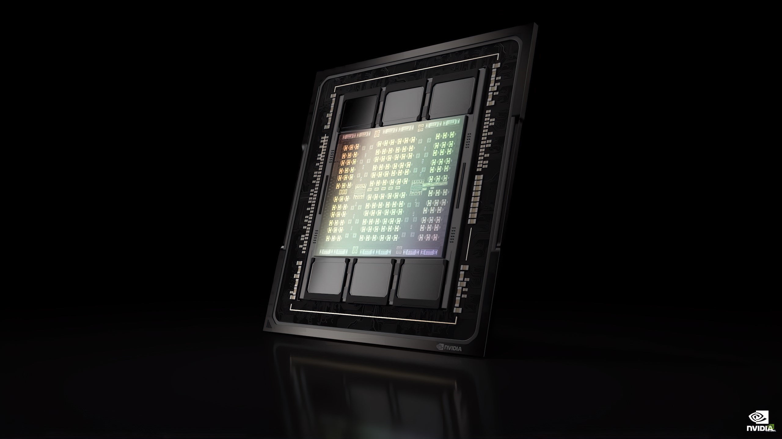
Today, HBM stacks integrate 8, 12 or 16 memory units as well as a logic layer that acts as a hub. HBM stacks are placed on the interposer next to CPUs or GPUs and connected to their processors using a 1024-bit interface. SK Hynix, on the other hand, aims to completely eliminate interconnects by embedding HBM4 stacks directly into processors.
In fact, we have been experiencing something similar for a while. This approach is to some extent similar to AMD’s 3D V-Cache built directly into CPU dies, but HBM will of course have much higher capacities. Unlike 3D V-Cache, HBM will also be cheaper but slower in terms of performance.
SK Hynix is reportedly discussing the HBM4 integration design method with several fabless companies, including Nvidia. It is likely that SK Hynix and Nvidia will jointly design the chip from the beginning and manufacture it at TSMC, while TSMC will embed SK Hynix’s HBM4 memory into the logic chips using a wafer bonding technology.
There are some difficulties to overcome
 HBM4 memory will use a 2048-bit interface to connect to main processors, so intermediate components for HBM4 will be extremely complex and expensive. This makes it economically possible to directly connect memory and logic units. But while placing HBM4 stacks directly on logic chips will somewhat simplify chip designs and reduce costs, it will present another challenge: thermal.
Modern logic processors like Nvidia’s H100 consume hundreds of watts of power and emit hundreds of watts of thermal energy. The power consumption of HBM memories is not low either. So cooling a package containing both logic chips and memory will present new challenges.
While there are fundamental hurdles to overcome for now, integrating memory directly into processors will also change the way chips are designed and manufactured. Manufacturing DRAM using the same processing technology as the corresponding CPU or GPU will improve performance. In turn, memory costs will increase significantly. “Within 10 years, the ‘rules of the game’ for semiconductors may change and the distinction between memory and logic semiconductors may become irrelevant,” industry officials said.


 36885
36885


