
 As part of Intel Innovation 2023, the chipmaker shared in-depth details about its new Meteor Lake processors. Intel is making its biggest breakthrough in recent years with its Core Ultra “Meteor Lake” processors. With its completely new architecture and production technology, Intel will compete with AMD more fiercely than ever before in recent years.
Release date of Intel Core Ultra “Meteor Lake” processors
As part of the event, Intel will launch the Core Ultra series processors within the Meteor Lake family on December 14. The Meteor Lake family will first target the mobile side, that is, laptops. The new artificial intelligence chip will give processors unique capabilities.
Although the company did not share product-level details, it unveiled its new 3D performance hybrid architecture. Under the hood, CPU and GPU microkernel architectures, neural processing unit (NPU), Foveros 3D packaging technology, a new approach to power management and new cores emerged. Intel also shared details about its new EUV-enabled Intel 4 (7nm) process node, which the company says delivers the best initial throughput it’s seen in a decade.
The biggest architectural change in the last 40 years
 Intel says its new design methodology delivers dramatic gains in power efficiency, but it hasn’t yet shared performance benchmarks. Intel describes its transition to Foveros 3D technology as the biggest architectural change in the last 40 years. Intel has actually needed these changes for some time as it tries to regain the lead over its primary rival TSMC in process node technology and outpace its primary chip rival AMD with its new chiplet-based architecture.
Intel also has to compete against Apple, which is making a disruptive entry into the laptop market with faster, more power-efficient processors. Meteor Lake marks a fundamental rethinking of not only Intel’s processor design, but also its approach to manufacturing its processors. These are the company’s first mainstream chips to use silicon from a rival factory. Intel uses TSMC’s process node technologies for three of the four active tiles in the processor (Intel calls them tiles, which can also be used as a tile design or chip).
| Meteor Lake chiplet/tile | Production process |
|---|---|
| Compute (CPU) | Intel / ‘Intel 4’ |
| Graphics (GPU) | TSMC/N5 (5nm) |
| SoC | TSMC/N6 (6nm) |
| I/O | TSMC/N6 (6nm) |
| 3D Foveros | Intel/22FFL (Intel 16) |
1st Generation Core Ultra Meteor Lake features
- Triple-Hybrid CPU Architecture (P/E/LP-E Cores)
- All-new Redwood Cove (P-Core)
- All-new Crestmont (E-Core)
- Up to 14 cores (6+8) for H/P Series and up to 12 cores (4+8) for U Series CPUs
- Intel ‘Xe-MTL’ GPU up to 128 EU
- LPDDR5X-7467 and DDR5-5200
- Up to 96GB DDR5 and 64GB LPDDR5X
- NPU
- x8 Gen 5 line for discrete GPU (H Series Only)
- Triple x4 M.2 Gen 4 SSD support
- Four Thunderbolt 4 ports
We will discuss the details of these later in the article. First of all, we will talk about the details and architecture of these tiles, starting from the basic information.
Meteor Lake architecture
 First of all, Intel calls the cihplet (can also be used as chiplet) architecture that we see in AMD as “tiled”. There is not much technical difference between these two terminologies. Intel says ’tiled’ processors mean a chip that uses advanced packaging that enables parallel communication between chip units, while standard packaging uses a serial interface that is not as performance- or energy-efficient. However, other competing processors with advanced packaging are still referred to as chiplet-based. So the terms can be used interchangeably.
 Meteor Lake has four decoupled active tiles mounted on a passive interposer. These appear as Compute (CPU) tile, graphics (GPU) tile, SoC tile and I/O tile. The casting of the parts, which are all designed by Intel and have microarchitectures, is carried out in partnership with TSMC. While TSMC produces I/O, SoC and GPU tiles in processors, Intel produces CPU tiles in the Intel 4 process.
 All four tiles are positioned on top of Intel-manufactured Foveros 3D, which connects functional units with high bandwidth and low latency so that the chip operates as much as possible as a single monolithic die. Meteor Lake also has three computing units: CPU, NPU, and GPU, which can handle AI workloads. Now let’s take a closer look at these four tiles.
Meteor Lake CPU tile
 Intel builds the compute (CPU) tile with the Intel 4 manufacturing process. In this way, Intel can meet the special requirements it requires on the CPU side. As before, Intel uses a mix of P-core (performance) and E-core (efficiency). However, these two types of cores are now supported by two new low-power cores located in the SoC tile. These two new cores are designed for the lowest-power tasks, which we’ll cover in the SoC tile section below. Intel calls this new three-layer core hierarchy 3D performance hybrid architecture.
The CPU tile carries Redwood Cove P-Cores and Crestmont E-cores, and surprisingly there isn’t much improvement in IPC. In fact, although the Redwood Cove cores have some improvements, they do not provide an improvement in instructions per cycle (IPC) throughput. Intel says Redwood Cove resembles what it traditionally calls “tick,” meaning it’s essentially the same microarchitecture and IPC found in the Golden Cove and Raptor Cove microarchitectures used in the 12th and 13th generation Alder/Raptor Lake processors.
 Rather than relying on microarchitectural IPC gains, Intel uses a proven architecture to unlock the advantages of a more refined, smaller process; in this scenario, Intel 4. The new Intel 4 process provides better performance at any point on the voltage/frequency curve than the Intel 7 node previously used in Intel’s PC chips, meaning it can run faster at the same power level or run the same speed at lower power. Intel says it’s focused on achieving higher power efficiency with this design, so it’s clear we shouldn’t expect radical performance increases from P-cores. Intel says the Intel 4 process delivers a 20 percent improvement in power efficiency, which is impressive.
Intel has also made some fine touches to accommodate the new tiled design, such as improving memory and cache bandwidth at both a per-core and packet level, which could provide an extra boost in multi-threaded workloads.
 Intel’s Crestmont E-Core microarchitecture has a 3 percent IPC improvement over the previous generation Gracemont, but most of that is due to the addition of support for Vector Neural Network Instructions (VNNI), which improves performance in AI workloads. However, Crestmont has an important innovation: This Crestmont architecture can be arranged in clusters of two or four cores that share the E-cores’ 4MB L2 cache slice and 3MB L3 cache.
The previous generation Gracemont did not have this feature, so it could only use Intel E-cores in quad-core clusters. Now Intel can build smaller dual-core clusters with twice as much cache per core, and it’s taken exactly that approach for its lower-power E-cores on the SoC tile (which use the same Crestmont architecture as the standard E-cores on the compute die). but they are produced in the TSMC N6 process). As with previous generations, each E-core runs single-threaded. Intel has also doubled the L1 cache to 64KB.
Crestmont cores do not support AMX or AVX-512, but they do support AVX10. Intel hasn’t announced full details yet, but we do know that the Crestmont architecture supports the first revision of AVX10. Ultimately, this could allow Intel to add AVX-512 support back to P-core, as a system exists to allow those instructions to be routed solely to P-core. We’ll have to wait to find out whether Intel will fully embrace this approach. Crestmont also supports BF16, FP16, AVX-IFMA and AVX-DOT-PROD-INT8.
Meteor Lake GPU tile
 The GPU tile is produced on the TSMC N3 compute node and uses Intel’s Xe-LPG architecture; This architecture now has the same features as the Xe-HPG architecture found in Intel’s discrete graphics cards. Intel claims double the performance and performance per watt for this unit over the previous generation, among other key features.
 Intel has also gone for decoupling in the graphics tile by separating the Xe Media and Display engine blocks from the main engine on the GPU die and moving them to the SOC tile, which helps with power consumption in many scenarios. Naturally, the GPU tile is optimized for 3D performance, which includes hardware-accelerated ray tracing, mesh shading, variable rate shading, and sampler feedback.
 Intel also adjusted the graphics engine’s voltage and frequency curve to run at much lower voltages and achieve higher clock speeds. The GPU can also perform highly efficient AI operations using DP4A acceleration.
Meteor Lake SoC tile
 The SoC tile is being shaped on the TSMC N6 process process and serves as the central point of contact for next-generation single-core tiles. Due to the SoC tile’s focus on low power usage, Intel also calls it a low power island. The SoC tile comes with two new compute clusters, two low-power E-cores, and Intel’s Neural Processing Unit (NPU), which is used entirely for AI workloads, among many other units.
Intel has moved all media, display, and rendering blocks from the GPU engine to the SoC tile, which helps maximize power efficiency by allowing these functions to run on the SoC tile when the GPU is in a lower power state. Since the GPU tile is also manufactured on the more expensive TSMC N3 node, removing these non-performance-sensitive blocks allowed Intel to make better use of the more expensive transistors in the GPU tile for graphics computing. The SoC tile hosts display interfaces such as HDMI 2.1, DisplayPort 2.1, and DSC 1.2a, while also supporting 8K HDR and AV1 encoding/decoding.
 The SoC tile and the GPU tile are located side by side, and both tiles communicate via a die-to-die (tile-to-tile) interface. Each side of the interconnect has a primary baseband interface that provides the bandwidth required to transfer data between chips. This connection provides a much more efficient path than standard traces through organic substrates (such as PCBs) through the underlying Foveros 3D silicon.
 The GPU connects the NPU to an isolated high-performance cache-coherent network (NOC) that connects the low-power e-cores and media and display engines to ensure they can efficiently access the memory bandwidth provided by memory controllers on the same bus. This NOC is also connected to the computing (CPU) tile via another tile-to-tile interface on the other side of the tile.
Intel also has a second, lower-power IO Fabric that connects to the I/O tile via another tile-to-tile interface. This IO structure also includes other lower priority devices such as Wi-Fi 6E and 7, Bluetooth, security engines, ethernet, PCIe, SATA and the like.
 This leaves Intel with two independent structures on the die, but they must be able to communicate with each other. Intel chose to connect the two with an I/O Cache (IOC) that buffers the traffic between the two structures. Cross-communication between the two buses will likely introduce additional delay.
Intel calls this new structure hierarchy next generation Uncore. Intel has also now added an independent power management controller (PMC) to each tile for independent voltage and frequency control. But these are all connected to two PMCs that control independent structures in the SoC tile, thus creating a more energy-saving power management hierarchy.
Meteor Lake I/O tile
 Intel’s new generation uncore design methodology is not without its disadvantages. The SoC tile houses DDR5 memory and PCIe controllers, but these external interfaces can only be placed on two sides of the die – the other two sides are used for communication with other tiles. This imposes a limitation on the number of connections that can be placed on these edges (shoreline) of the pattern. To solve this problem, Intel created a secondary I/O tile to provide more space for connections to additional PCIe lanes and the Thunderbolt 4 external interface.
The I/O tile is the smallest of the four Meteor Lake tiles and is manufactured in the TSMC N6 process. This tile houses I/O functions such as Thunderbolt 4 (yes, not 5) and PCIe Gen 5.0. Intel will use different sizes of I/O tiles for different products depending on the amount of connectivity required.
Low power E-core
 Intel’s SoC tile comes with two low-power E-cores that use the same Crestmont microarchitecture that we described in the compute tile section. These low-power cores can run the operating system in certain light-use modes, such as when playing video, so that the entire CPU tile is put into low-power mode to save energy. Additionally, these cores can handle most daily light background tasks that do not require the weight of quad-core E-core clusters on the CPU tile, thus putting individual cores to sleep more frequently. Intel hasn’t shared details about the performance of these cores, but we do know that they are specifically optimized for TSMC’s low-power N6 node.
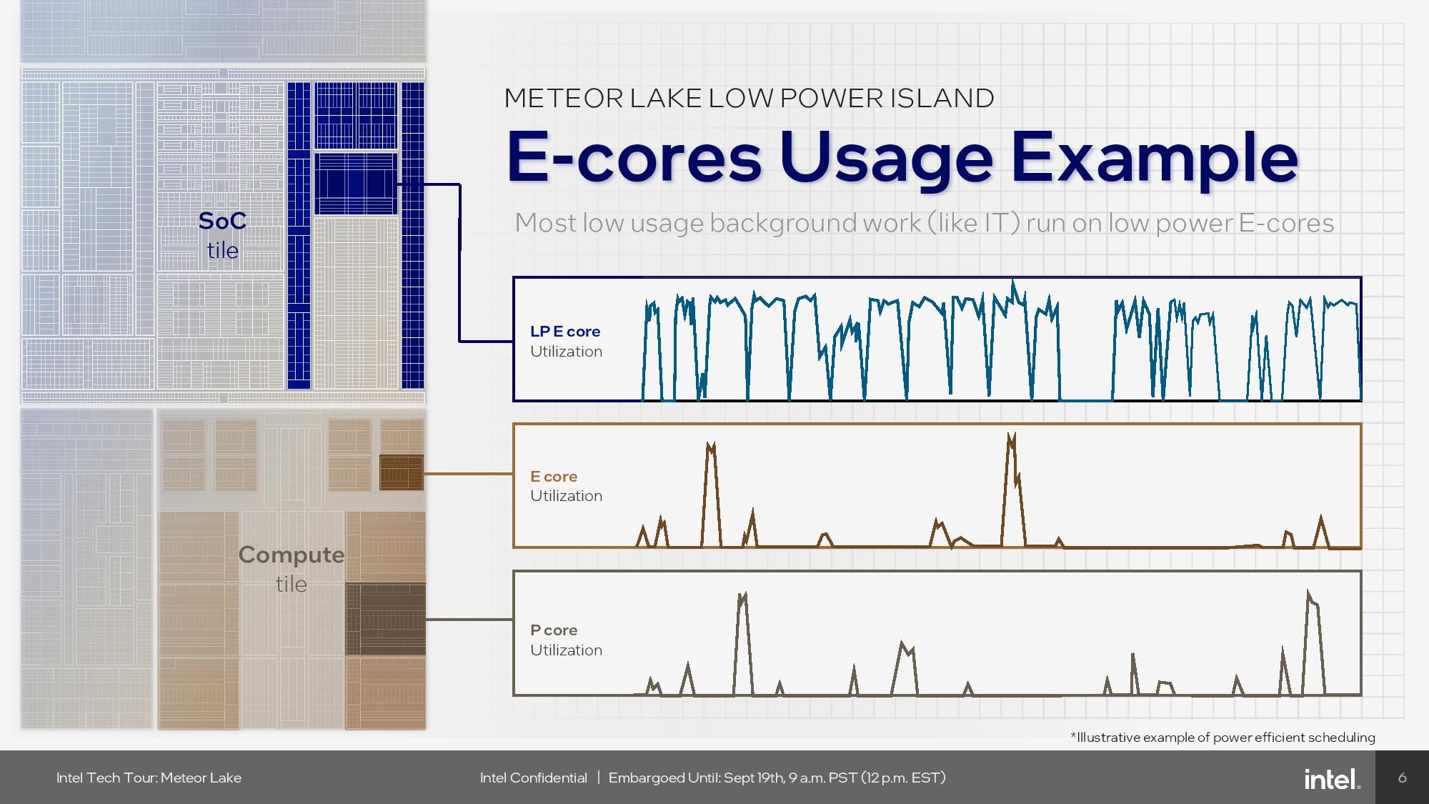 However, if a thread starts running on low-power E-cores and turns out to need more processing power, the operating system will transfer it to a faster core. Intel has historically prioritized P-cores as a primary target for any workload. It will be necessary to look at the impact of this decision to prioritize low-power E-cores on performance sensitivity.
Neural Processing Unit (NPU)
 Intel’s neural processing unit (NPU) is a dedicated AI engine designed specifically to run continuous AI inference workloads (not training), but Meteor Lake also includes the CPU, GPU, and GNA engine that can run a variety of other AI workloads. The NPU is used primarily for background tasks, while the GPU comes into play for more heavily parallelized tasks.
Some AI workloads can run on both the NPU and GPU simultaneously, and Intel has mechanisms in place that allow developers to target different compute layers based on the needs of the application at hand.
This will ultimately enable higher performance with lower power (8 times less, in fact), which is one of the main goals of using the AI acceleration NPU.
 Many of today’s more intensive AI workloads, such as training ChatGPT and similar large language models, require intense compute horsepower and will continue to run in data centers. However, Intel says some AI applications, such as audio, video and image processing, will be handled natively on the computer, improving latency, privacy and cost.
In addition to DIrectML, Intel’s NPU also supports ONNX and OpenVINO, which Intel says offers better performance on its silicon.
The nascent PC AI software ecosystem is now moving faster to adapt to new custom AI engines found not only in Intel’s chips, but also in AMD’s rival Ryzen 7040 series processors, which have their own custom AI engines. Intel plans to bring its NPU to tens of millions of devices by 2025, and we can expect the process to accelerate as AMD makes similar design decisions. Simply put, we will see more native AI applications on devices.
Foveros 3D
 Advances in packaging and interconnect are rapidly changing the face of modern processors. Both are now as important as the underlying compute node technology. In some ways they are arguably even more important, as they allow mixing and matching different types of compute nodes within a single package to achieve the best blend of performance, power consumption and cost.
Intel manufactures the Foveros interposer using the low-cost and low-power optimized 22FFL process. Intel places four Meteor Lake tiles on top of a passive Foveros 3D interposer/base tile, then the tiles and interposer are fused together with microbump connections that enable high-speed communication and efficient power distribution.
 Since the passive interposer does not have any logic, it does not perform any operations and mostly serves as a high-speed path for communication between tiles. However, it has embedded MIM capacitors that help ensure stable power delivery to the tiles during heavy load periods.
Foveros, on the other hand, is in the early stages of development according to Intel. For now Foveros enables up to 770 microbumps per square millimeter, but this will improve greatly in the future: the Foveros roadmap includes steps of 25 and 18 microns in future designs. Intel says it could even use hybrid bonding interconnects (HBI) to theoretically achieve 1-micron pitches in the future.
 Intel says the Foveros interconnect/underlay supports up to 160 GB/s per mm, so bandwidth will scale with additional interconnects. Therefore, Foveros does not suffer from significant bandwidth or latency constraints that require design compromises.
At the end of the day, advanced packaging technology is used to mimic the key performance and strength characteristics of a monolithic mold. Intel thinks Foveros is the winning formula that meets these goals.
Foveros technology offers:
- Low voltage CMOS interface
- High bandwidth, low latency
- Synchronous and asynchronous signaling
- Low space usage
Intel 4 process process
 The health of the Intel 4, Intel’s first node produced with EUV, is critically important as the company tries to recover from years of missteps in process technology. Highlights include doubling high-performance transistor scaling over the end node and 20 percent higher clock speeds at the same power threshold. Intel chose to focus on power efficiency rather than performance on this node. By the way, Intel 4 corresponds to 7nm.
last words
Intel said its long-awaited Intel 4 process yielded better than expected, signaling that the company has a solid foundation on which to build its next-generation Core Ultra ‘Meteor Lake’ processors. While the addition of the tile/chiplet architecture provides opportunities to reduce costs and increase performance, it is a turning point for the company as it will be the first time Intel will use this type of design. In the next steps to be taken, further development can be expected.
With a massive re-architecture of components, disruptive 3D Foveros packaging technology, and a focus on boosting AI workloads, the new Meteor Lake chips look promising. While Intel is coy about performance metrics and SKU details, it says it delivers a 20 percent improvement in power efficiency, which could give it a better position against rival laptop chips from AMD and Apple, which currently lead in these metrics. Meteor Lake will be released on December 14, 2023.


 4290
4290


